- 您现在的位置:买卖IC网 > Sheet目录17360 > IRDC3475 (International Rectifier)BOARD EVAL SUPIRBUCK IR3475
10A ? Highly ? Integrated ? SupIRBuck TM ?
IR3475 ?
STABILITY ? CONSIDERATIONS ??
Constant ‐ on ‐ time ? control ? is ? a ? fast, ? ripple ? based ? control ?
scheme. ? Unstable ? operation ? can ? occur ? if ? certain ? conditions ?
are ? not ? met. ? The ? system ? instability ? is ? usually ? caused ? by: ?
Switching ? noise ? coupled ? to ? FB ? input: ??
This ? causes ? the ? PWM ? comparator ? to ? trigger ? prematurely ?
after ? the ? 500ns ? minimum ? on ‐ time ? for ? lower ? MOSFET. ??
It ? will ? result ? in ? double ? or ? multiple ? pulses ? every ? switching ?
cycle ? instead ? of ? the ? expected ? single ? pulse. ? Double ? pulsing ?
can ? causes ? higher ? output ? voltage ? ripple, ? but ? in ? most ?
application ? it ? will ? not ? affect ? operation. ? This ? can ? usually ? be ?
prevented ? by ? careful ? layout ? of ? the ? ground ? plane ? and ? the ??
FB ? sensing ? trace. ?
Steady ? state ? ripple ? on ? FB ? pin ? being ? too ? small: ??
The ? PWM ? comparator ? in ? IR3475 ? requires ? minimum ??
7mVp ‐ p ? ripple ? voltage ? to ? operate ? stably. ? Not ? enough ? ripple ?
will ? result ? in ? similar ? double ? pulsing ? issue ? described ? above. ?
Solving ? this ? may ? require ? using ? output ? capacitors ? with ?
higher ? ESR. ??
ESR ? loop ? instability: ??
The ? stability ? criteria ? of ? constant ? on ‐ time ? is: ??
LAYOUT ? RECOMMENDATIONS ?
Bypass ? Capacitor: ??
As ? VCC ? bypass ? capacitor, ? a ? 1μF ? high ? quality ? ceramic ?
capacitor ? should ? be ? placed ? on ? the ? same ? side ? as ? the ? IR3475 ?
and ? connected ? to ? VCC ? and ? PGND ? pins ? directly. ? A ? 1μF ?
ceramic ? capacitor ? should ? be ? connected ? from ? 3VCBP ? to ?
GND ? to ? avoid ? noise ? coupling ? into ? controller ? circuits. ? For ?
single ‐ ground ? designs, ? a ? resistor ? (R12) ? in ? the ? range ? of ? 5 ? to ?
10 Ω? in ? series ? with ? the ? 1μF ? capacitor ? as ? shown ? in ? Figure ? 4 ? is ?
recommended. ??
Boot ? Circuit: ??
C BOOT ? should ? be ? placed ? near ? the ? BOOT ? and ? PHASE ? pins ? to ?
reduce ? the ? impedance ? when ? the ? upper ? MOSFET ? turns ? on. ??
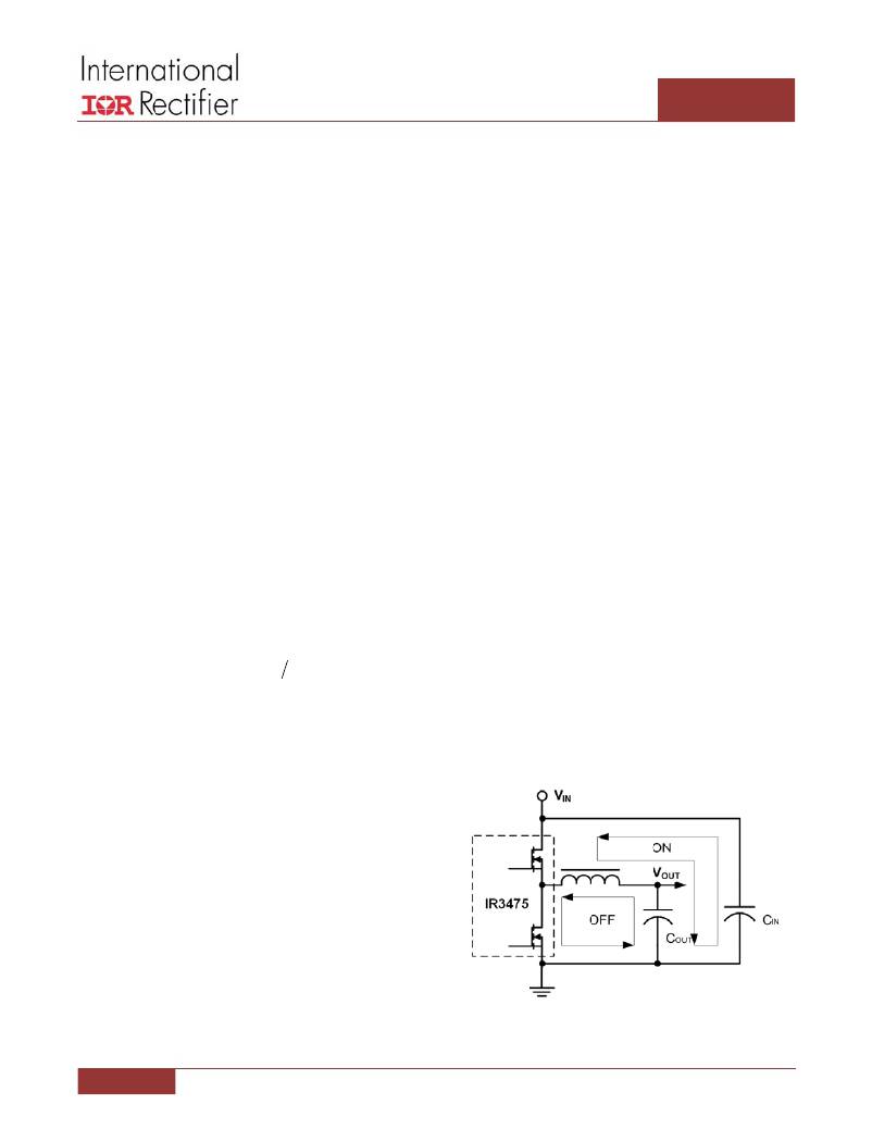
Power ? Stage: ??
Figure ? 30 ? shows ? the ? current ? paths ? and ? their ? directions ??
for ? the ? on ? and ? off ? periods. ? The ? on ? time ? path ? has ? low ?
average ? DC ? current ? and ? high ? AC ? current. ?? Therefore, ? it ? is ?
recommended ? to ? place ? the ? input ? ceramic ? capacitor, ? upper, ?
and ? lower ? MOSFET ? in ? a ? tight ? loop ? as ? shown ? in ? Figure ? 30. ??
The ? purpose ? of ? the ? tight ? loop ? from ? the ? input ? ceramic ?
capacitor ? is ? to ? suppress ? the ? high ? frequency ? (10MHz ? range) ?
switching ? noise ? and ? reduce ? Electromagnetic ? Interference ?
?
?
ESR ? C OUT > T ON 2
(EMI). ?? If ? this ? path ? has ? high ? inductance, ? the ? circuit ? will ?
cause ? voltage ? spikes ? and ? ringing, ? and ? increase ? the ?
switching ? loss. ? The ? off ? time ? path ? has ? low ? AC ? and ? high ?
average ? DC ? current. ? Therefore, ? it ? should ? be ? laid ? out ? with ??
If ? ESR ? is ? too ? small ? that ? this ? criteria ? is ? violated ? then ? sub ‐
harmonic ? oscillation ? will ? occur. ? This ? is ? similar ? to ? the ?
instability ? problem ? of ? peak ‐ current ‐ mode ? control ? with ?
D>0.5. ? Increasing ? ESR ? is ? the ? most ? effective ? way ? to ? stabilize ?
the ? system, ? but ? the ? tradeoff ? is ? the ? larger ? output ? voltage ?
ripple. ??
System ? with ? all ? ceramic ? output ? capacitors: ??
For ? applications ? with ? all ? ceramic ? output ? capacitors, ? the ? ESR ?
is ? usually ? too ? small ? to ? meet ? the ? stability ? criteria. ? In ? these ?
applications, ? external ? slope ? compensation ? is ? necessary ? to ?
make ? the ? loop ? stable. ? The ? ramp ? injection ? circuit, ? composed ?
of ? R6, ? C13, ? and ? C14, ? shown ? in ? Figure ? 4 ? is ? required. ??
The ? inductor ? current ? ripple ? sensed ? by ? R6 ? and ? C13 ? is ? AC ?
coupled ? to ? the ? FB ? pin ? through ? C14. ? C14 ? is ? usually ? chosen ?
between ? 1 ? to ? 10nF, ? and ? C13 ? between ? 10 ? to ? 100nF. ? R6 ?
should ? then ? be ? chosen ? such ? that ? L/DCR ? = ? C13*R6. ??
a ? tight ? loop ? and ? wide ? trace ? at ? both ? ends ? of ? the ? inductor. ?
Lowering ? the ? loop ? resistance ? reduces ? the ? power ? loss. ? The ?
typical ? resistance ? value ? of ? 1 ‐ ounce ? copper ? thickness ? is ?
0.5m Ω? per ? square ? inch. ?
Q1
Q2
?
Figure ? 30: ? Current ? Path ? of ? Power ? Stage ?
17
March ? 27, ? 2013 ?? | ?? V2.2 ?? | ?? PD97602
发布紧急采购,3分钟左右您将得到回复。
相关PDF资料
RO-2415S/H
CONV DC/DC 1W 24VIN 15VOUT
IRDC3863
BOARD EVAL SUPIRBUCK IR3863
IRDC3476
BOARD EVAL SUPIRBUCK IR3476
RO-243.3S/H
CONV DC/DC 1W 24VIN 3.3VOUT
RO-2424S/H
CONV DC/DC 1W 24VIN 24VOUT
MIC2545A-1BTS
IC SW CURR LIMIT HI SIDE 14TSSOP
MIC2545A-1BN
IC SW CURR LIMIT HI SIDE 8-DIP
RO-2412S/H
CONV DC/DC 1W 24VIN 12VOUT
相关代理商/技术参数
IRDC3476
功能描述:电源管理IC开发工具 9999V 999A POL IC RoHS:否 制造商:Maxim Integrated 产品:Evaluation Kits 类型:Battery Management 工具用于评估:MAX17710GB 输入电压: 输出电压:1.8 V
IRDC3477
功能描述:电源管理IC开发工具 9999V 999A POL IC RoHS:否 制造商:Maxim Integrated 产品:Evaluation Kits 类型:Battery Management 工具用于评估:MAX17710GB 输入电压: 输出电压:1.8 V
IRDC3621
功能描述:电源管理IC开发工具 RoHS:否 制造商:Maxim Integrated 产品:Evaluation Kits 类型:Battery Management 工具用于评估:MAX17710GB 输入电压: 输出电压:1.8 V
IRDC3622D
功能描述:电源管理IC开发工具 IRDC3622D Eval BRD IRF6629 DIRECTFET RoHS:否 制造商:Maxim Integrated 产品:Evaluation Kits 类型:Battery Management 工具用于评估:MAX17710GB 输入电压: 输出电压:1.8 V
IRDC3622S
功能描述:电源管理IC开发工具 IRF6622 IRF6678 FET Ref Design Guide RoHS:否 制造商:Maxim Integrated 产品:Evaluation Kits 类型:Battery Management 工具用于评估:MAX17710GB 输入电压: 输出电压:1.8 V
IRDC3624
制造商:International Rectifier 功能描述:HIGH PERFORMANCE SYNCHRONOUS BUCK CONTROLLER EVAL BOARD - Bulk 制造商:International Rectifier 功能描述:EVAL BOARD FOR IR3624
IRDC3628
制造商:International Rectifier 功能描述:TUBE / 9999V 999.000A LVIC OTHER
IRDC3629
功能描述:电源管理IC开发工具 IR3629 Eval BRD 600kHz Controller RoHS:否 制造商:Maxim Integrated 产品:Evaluation Kits 类型:Battery Management 工具用于评估:MAX17710GB 输入电压: 输出电压:1.8 V
